- 您现在的位置:买卖IC网 > Sheet目录1992 > DAC8562FP (Analog Devices Inc)IC DAC 12BIT PARALLEL 5V 20-DIP
DAC8562
REV. A
–14–
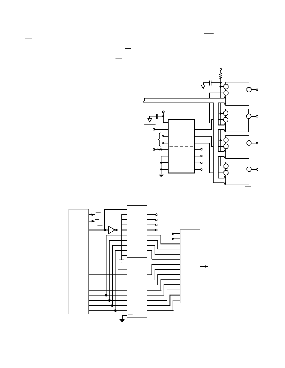
Decoding Multiple DAC8562s
The CE function of the DAC8562 can be used in applications
to decode a number of DACs. In this application, all DACs re-
ceive the same input data; however, only one of the DACs’ CE
input is asserted to transfer its parallel input register contents
into the DAC. In this circuit, shown in Figure 40, the CE tim-
ing is generated by a 74HC139 decoder and should follow the
DAC8562’s standard timing requirements. To prevent timing
errors, the 74HC139 should not be activated by its ENABLE
input while the coded address inputs are changing. A simple
timing circuit, R1 and C1, connected to the DACs’ CLR pins
resets all DAC outputs to zero during power-up.
MICROPROCESSOR INTERFACING
DAC-8562–MC68HC11 INTERFACE
The circuit illustrated in Figure 41 shows a parallel interface be-
tween the DAC8562 and a popular 8-bit microcontroller, the
M68HC11, which is configured in a single-chip operating
mode. The interface circuit consists of a pair of 74ACT11373
transparent latches and an inverter. The data is loaded into the
latches in two 8-bit bytes; the first byte contains the four most
significant bits, and the lower 8 bits are in the second byte. Data
is taken from the microcontroller’s port B output lines, and
three interface control lines, CLR, CE, and MSB/LSB, are con-
trolled by the M68HC11's PC2, PC1, and PC0 output lines, re-
spectively. To transfer data into the DAC, PC0 is set, enabling
U1’s outputs. The first data byte is loaded into U1 where the
four least significant bits of the byte are connected to
MSB–DB8. PC0 is then cleared; this latches U1’s inputs and
enables U2’s outputs. U2s outputs now become DB7–DB0.
The DAC output is updated with the contents of U1 and U2
when PC1 is cleared. The DAC’s CLR input, controlled by the
M68HC11’s PC2 output line, provides an asynchronous clear
function that sets the DAC’s output to zero. Included in this sec-
tion is the source code for operating the DAC-8562–M68HC11
interface.
VCC
1G
1A
1B
2G
2A
2B
GND
1Y0
1Y1
1Y2
1Y3
2Y0
2Y1
2Y2
2Y3
12
1k
+5V
16
1
2
3
15
14
13
8
11
10
9
7
6
5
4
NC
0.1F
+5V
ENABLE
CODED
ADDRESS
+5V
C1
0.1F
R1
1k
15
DAC-8562
#4
13
16
15
16 DAC-8562
#1
13
15
DAC-8562
#2
13
15
DAC-8562
#3
13
16
VOUT1
VOUT3
VOUT4
VOUT2
DATA
74HC139
Figure 40. Decoding Multiple DAC8562s Using the CE Pin
13
23
22
21
20
1
16
15
14
24
1
2
3
4
9
10
11
12
U1
C
1D
2D
3D
4D
5D
6D
7D
8D
OC
1Q
2Q
3Q
4Q
5Q
6Q
7Q
8Q
13
23
22
21
20
1
16
15
14
24
1
2
3
4
9
10
11
12
U2
C
1D
2D
3D
4D
5D
6D
7D
8D
OC
1Q
2Q
3Q
4Q
5Q
6Q
7Q
8Q
CLR
CE
MSB/ LSB
15
16
9
8
7
6
5
4
3
2
U3
CLR
CE
MSB
DB10
DB9
DB8
DB7
DB6
DB5
DB4
1
19
18
17
DB3
DB2
DB1
LSB
NC
PC2
PC1
74ACT11373
*DAC-8562
74ACT11373
VOUT
74HC04
*M6BHC11
PC2
PC1
PC0
PB7
PB6
PB5
PB4
PB3
PB2
PB1
PB0
*ADDITIONAL PINS OMITTED FOR CLARITY
1
2
13
Figure 41. DAC8562 to MC68HC11 Interface
发布紧急采购,3分钟左右您将得到回复。
相关PDF资料
DS1004Z-5+T
IC DELAY LINE 5TAP 25NS 8-SOIC
DS1005-125+
IC DELAY LINE 5TAP 125NS 14-DIP
DS1007S-2+T&R
IC DELAY LINE 4NS 16-SOIC
DS1010S-50+T&R
IC DELAY LINE 10TAP 16-SOIC
DS1013S-25+T&R
IC DELAY LINE 25NS 16-SOIC
DS1020S-50+T
IC DELAY LINE 256TAP 16-SOIC
DS1021S-50+T&R
IC DELAY LINE 256TAP 16-SOIC
DS1023S-25+W
IC DELAY LINE 256TAP 16-SOIC
相关代理商/技术参数
DAC8562FPZ
功能描述:IC DAC 12BIT PARALLEL 5V 20-DIP RoHS:是 类别:集成电路 (IC) >> 数据采集 - 数模转换器 系列:- 产品培训模块:Lead (SnPb) Finish for COTS
Obsolescence Mitigation Program 标准包装:50 系列:- 设置时间:4µs 位数:12 数据接口:串行 转换器数目:2 电压电源:单电源 功率耗散(最大):- 工作温度:-40°C ~ 85°C 安装类型:表面贴装 封装/外壳:8-TSSOP,8-MSOP(0.118",3.00mm 宽) 供应商设备封装:8-uMAX 包装:管件 输出数目和类型:2 电压,单极 采样率(每秒):* 产品目录页面:1398 (CN2011-ZH PDF)
DAC8562FR
制造商:未知厂家 制造商全称:未知厂家 功能描述:12-Bit Digital-to-Analog Converter
DAC8562FRU
功能描述:IC DAC 12BIT PARALLEL 5V 20TSSOP RoHS:否 类别:集成电路 (IC) >> 数据采集 - 数模转换器 系列:- 产品培训模块:Data Converter Fundamentals
DAC Architectures 标准包装:750 系列:- 设置时间:7µs 位数:16 数据接口:并联 转换器数目:1 电压电源:双 ± 功率耗散(最大):100mW 工作温度:0°C ~ 70°C 安装类型:表面贴装 封装/外壳:28-LCC(J 形引线) 供应商设备封装:28-PLCC(11.51x11.51) 包装:带卷 (TR) 输出数目和类型:1 电压,单极;1 电压,双极 采样率(每秒):143k
DAC8562FRU-REEL7
功能描述:IC DAC 12BIT PARALLEL 5V 20TSSOP RoHS:否 类别:集成电路 (IC) >> 数据采集 - 数模转换器 系列:- 产品培训模块:Data Converter Fundamentals
DAC Architectures 标准包装:750 系列:- 设置时间:7µs 位数:16 数据接口:并联 转换器数目:1 电压电源:双 ± 功率耗散(最大):100mW 工作温度:0°C ~ 70°C 安装类型:表面贴装 封装/外壳:28-LCC(J 形引线) 供应商设备封装:28-PLCC(11.51x11.51) 包装:带卷 (TR) 输出数目和类型:1 电压,单极;1 电压,双极 采样率(每秒):143k
DAC8562FRUZ
功能描述:IC DAC 12BIT PARALLEL 5V 20TSSOP RoHS:是 类别:集成电路 (IC) >> 数据采集 - 数模转换器 系列:- 产品培训模块:Data Converter Fundamentals
DAC Architectures 标准包装:750 系列:- 设置时间:7µs 位数:16 数据接口:并联 转换器数目:1 电压电源:双 ± 功率耗散(最大):100mW 工作温度:0°C ~ 70°C 安装类型:表面贴装 封装/外壳:28-LCC(J 形引线) 供应商设备封装:28-PLCC(11.51x11.51) 包装:带卷 (TR) 输出数目和类型:1 电压,单极;1 电压,双极 采样率(每秒):143k
DAC8562FS
功能描述:IC DAC 12BIT PARALLEL 5V 20-SOIC RoHS:否 类别:集成电路 (IC) >> 数据采集 - 数模转换器 系列:- 产品培训模块:Data Converter Fundamentals
DAC Architectures 标准包装:750 系列:- 设置时间:7µs 位数:16 数据接口:并联 转换器数目:1 电压电源:双 ± 功率耗散(最大):100mW 工作温度:0°C ~ 70°C 安装类型:表面贴装 封装/外壳:28-LCC(J 形引线) 供应商设备封装:28-PLCC(11.51x11.51) 包装:带卷 (TR) 输出数目和类型:1 电压,单极;1 电压,双极 采样率(每秒):143k
DAC8562FS-REEL
功能描述:IC DAC 12BIT PARALLEL 5V 20-SOIC RoHS:否 类别:集成电路 (IC) >> 数据采集 - 数模转换器 系列:- 产品培训模块:Data Converter Fundamentals
DAC Architectures 标准包装:750 系列:- 设置时间:7µs 位数:16 数据接口:并联 转换器数目:1 电压电源:双 ± 功率耗散(最大):100mW 工作温度:0°C ~ 70°C 安装类型:表面贴装 封装/外壳:28-LCC(J 形引线) 供应商设备封装:28-PLCC(11.51x11.51) 包装:带卷 (TR) 输出数目和类型:1 电压,单极;1 电压,双极 采样率(每秒):143k
DAC8562FSZ
功能描述:IC DAC 12BIT PARALLEL 5V 20SOIC RoHS:是 类别:集成电路 (IC) >> 数据采集 - 数模转换器 系列:- 标准包装:1 系列:- 设置时间:4.5µs 位数:12 数据接口:串行,SPI? 转换器数目:1 电压电源:单电源 功率耗散(最大):- 工作温度:-40°C ~ 125°C 安装类型:表面贴装 封装/外壳:8-SOIC(0.154",3.90mm 宽) 供应商设备封装:8-SOICN 包装:剪切带 (CT) 输出数目和类型:1 电压,单极;1 电压,双极 采样率(每秒):* 其它名称:MCP4921T-E/SNCTMCP4921T-E/SNRCTMCP4921T-E/SNRCT-ND